
 Flexible Wearable Electronics Advance Research


CASPaR Lab
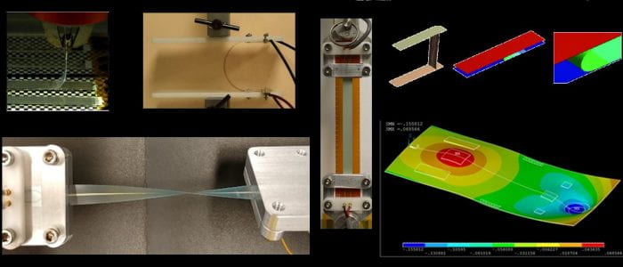
CASPaR Lab’s research is in the areas of micro- and nano-scale structure fabrication, characterization, physics-based modeling and reliable design intended for various applications: aerospace and defense, automotive, computers and telecommunications, portable electronics, and medical. Members of Dr. Sitaraman’s group collaborate with various partners in both academia and industry, solving interdisciplinary research problems involving design, fabrication, experimentation, and computer modelling for packaged electronics. The lab’s recent research focuses on the development and standardization of novel electromechanical methods for testing, characterizing, and modeling of 3D printed, flexible, stretchable, and wearable electronics, such as IoT sensors, human performance monitors, and flexible antennas.
The CASPaR Lab’s past emphases of research have involved many other facets of electromechanical packaging reliability. In particular, past research included developing micro-scale and nano-scale structures that can be used as compliant packaging interconnects as well as bio-assays for disease diagnosis and to determine the efficacy of drug treatment. The research has also involved developing innovative stressed super layer techniques to determine the interfacial strength of thin structures ranging from 5 nm to 1-2 um. Mechanical characterization of thin-film structures is also being done using nano-indentation. CASPaR Lab’s research also aims to understand the long-term reliability of lead-based and lead-free solder interconnects through thermo-mechanical modeling, material microstructure evolution, reliability experiments, and laser moiré interferometry. In parallel, the research focuses on the next-generation integrated substrates that have high-density interconnects and microvias, embedded passives, and optoelectronic waveguides. In particular, Dr. Sitaraman’s group has done work in material length scale effects for microvia reliability, high-modulus and low-coefficient of thermal expansion (CTE) base substrate for thin-film processing, cure kinetics and interlayer dielectric cracking and delamination, reliability modeling and experiments for embedded passives, and refractive index stability, misalignment, spectral absorption, and reliability of optical waveguides.